Introduction
The Vivado Design Suite is a comprehensive development environment from Xilinx, designed to streamline the design, integration, and implementation of systems using Xilinx UltraScale, 7 series devices, and the Zynq-7000 family. With powerful tools like the IP Integrator and seamless integration with Vitis for software development, Vivado enables rapid prototyping and efficient design workflows. In this article, we’ll walk through creating a simple “Hello World” project on the Aller AU-Plus FPGA Board, using a 32-bit MicroBlaze soft processor and AXI4-connected peripherals.
What is MicroBlaze?
MicroBlaze is a 32-bit soft processor IP developed by Xilinx for their mid and high-end FPGA devices. It is compatible with Xilinx’s Ultrascale+, 6 and 7 series FPGAs. More information on MicroBlaze can be found on Xilinx’s MicroBlaze page. Advanced knowledge of MicroBlaze or AXI is not a prerequisite to follow this article. Thanks to the excellent tools provided by Xilinx, most of the design can be done without writing any code at all.
What is AXI?
AXI stands for Advanced eXtensible Interface. AXI is a bus interconnect based on ARM’s popular AMBA bus architecture. In a MicroBlaze system, AXI connects the microprocessor to all peripherals in the system. The only exception is the Block RAM which is attached to the processor through the LMB (Local Memory Bus). AXI4-Lite is available for connecting low throughput peripherals to the system such as the UART, GPIO, etc. AXI4-Lite uses fewer logic resources on FPGA compared to AXI. Usually, AXI is used to connect high throughput peripherals such as DDR memory, Ethernet, etc. Again, a detailed understanding of AXI is not required for following this article. But for curious readers, AXI Reference Guide is available here.
Aller AU-Plus FPGA Board with M.2 Interface
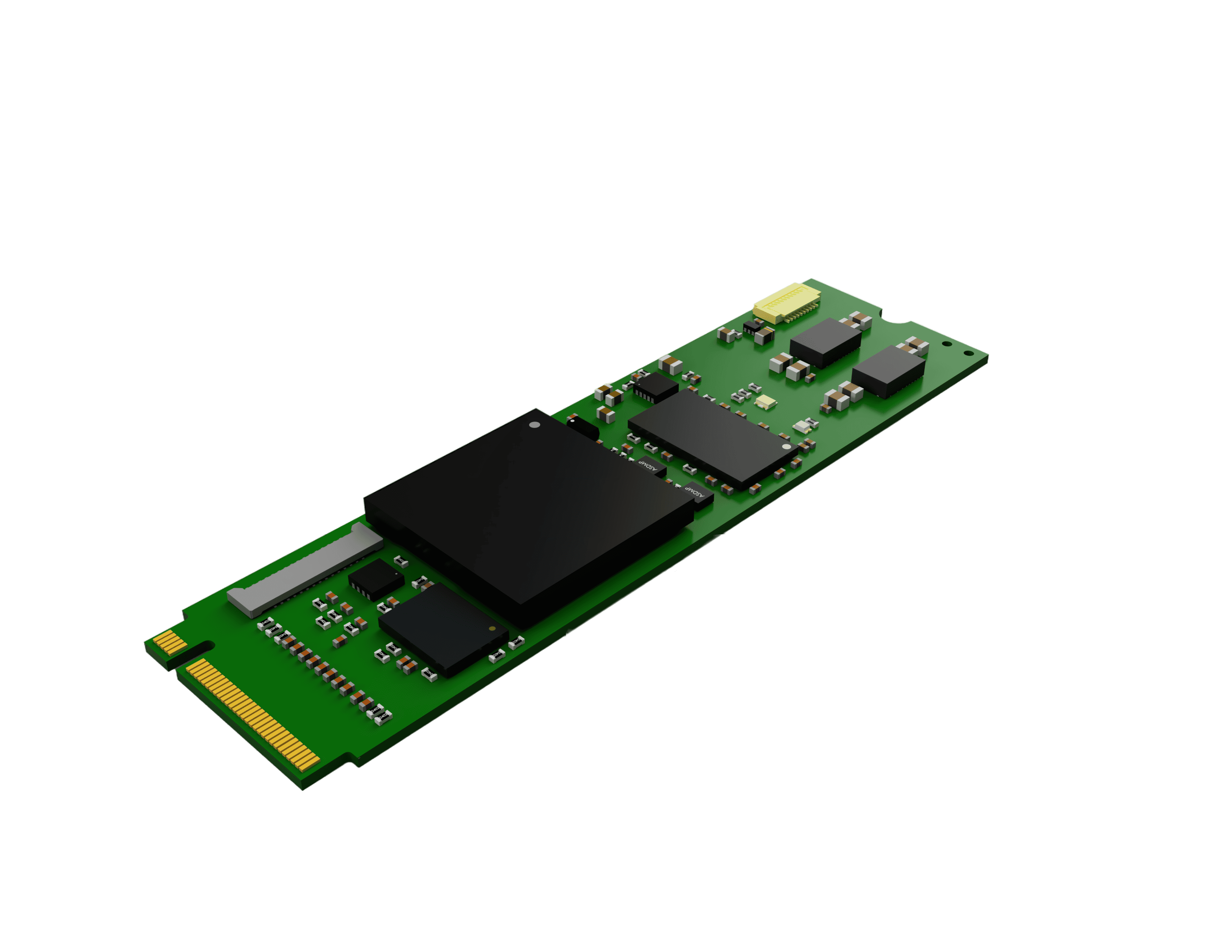
The Aller AU-Plus board from Numato Lab is an Artix Ultrascale Plus based development board designed to ease accelerated computing. It features an M.2 form factor M-key slot which is a computer storage interface based on the PCI Express standard. Thus Aller can be used with laptops, desktops, and servers seamlessly through its M.2 interface. This article will serve as a quick start guide for you to get familiar with Aller. Let’s get started!
Prerequisites:
Hardware:
- Aller AU-Plus FPGA Module
- Aller AU-Plus Carrier
- Xilinx Platform Cable USB
- USB type C cable
Software:
- Vivado Design Suite with Vitis version 2024.1
- Serial Terminal (PuTTY, Tera Term, etc.)
Creating MicroBlaze based Hardware Platform for Aller AU-Plus
The following steps will walk you through the process of creating a new project with Vivado and building a hardware platform with a MicroBlaze soft processor using the Vivado IP integrator. Screenshots are added wherever possible to make the process easier for the reader.
Step 1:
Download and install the Vivado Board Support Package files for Aller from here. Follow the README.md file on how to install Vivado board support files for Numato Lab boards.
Step 2:
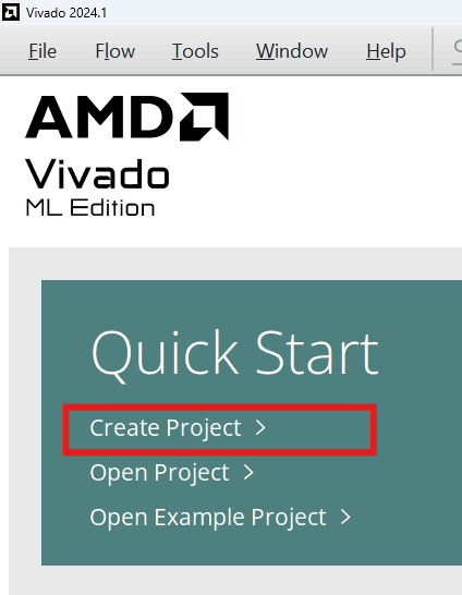
Start Vivado Design Suite, and select “Create Project” from Quick Start section. The project wizard will pop up. Press “next” to proceed with creating the project.
Step 3:
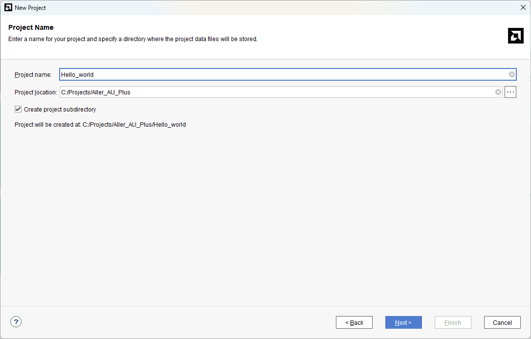
In the “Project Name” window, enter a name for the project and save it at a suitable location. Select the option “Create project subdirectory” to keep all the project files in a single folder and click “Next” without making any changes until you see the “Default Part” page.
Step 4:
In the “Default Part” window, select the “Boards” tab. Choose the Vendor as “numato.com”, filter the Name “Aller_AU_Plus” and select the board as shown below. If Aller_AU_Plus is not displayed in the Boards list, make sure that the board support files are installed correctly.
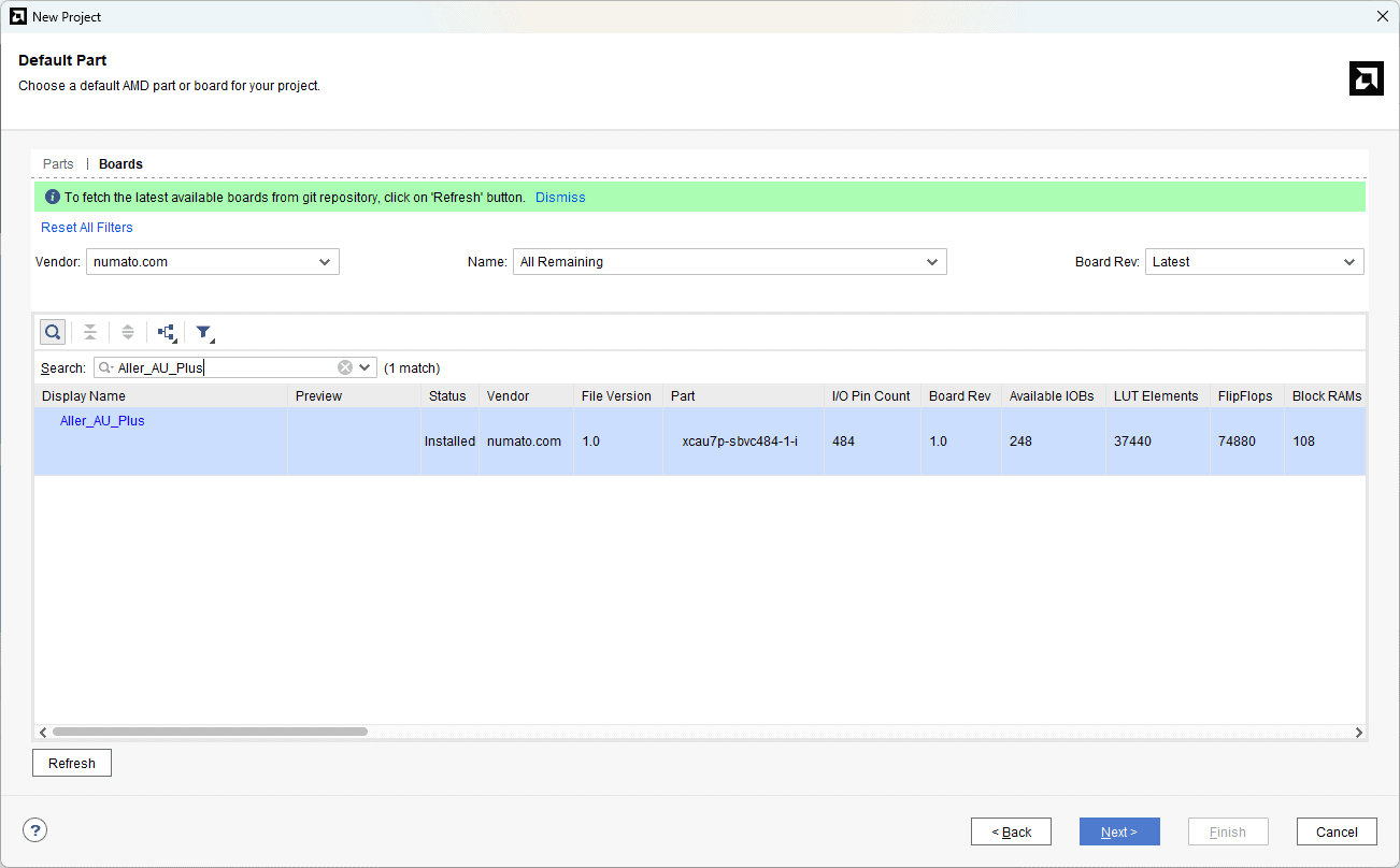
Click “Next” to continue. On the next page, click “Finish” to complete creating a new project. A new project will be created by Vivado with the selected settings.
Step 5:
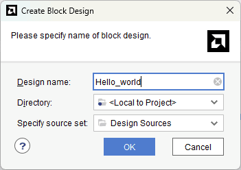
Under the “Flow Navigator” panel, click “Create Block Design” under the IP Integrator section. Enter a name for the block design and click “OK”.
An empty block design will be created.
Step 6:
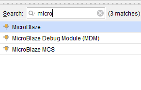
As shown in the “Diagram” window, click the “Add IP” icon, search for MicroBlaze and add it to the design by double-clicking its name in the list.
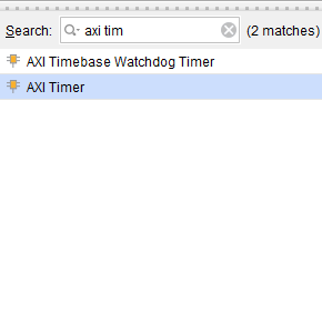
 Add AXI Timer to the block design.
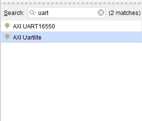
Similarly, add AXI Uartlite to the block design.
Step 7:
Click the “Board” tab. The default peripherals available for the Aller board will be listed as shown below.
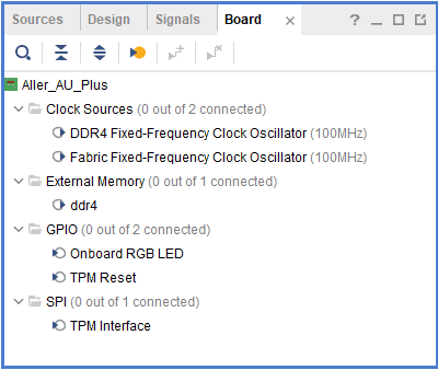
Drag and drop the Fabric Fixed-Frequency Clock Oscillator and ddr4 peripherals into the block design.
Step 8:
Click “Run Block Automation” and change the settings as shown below. Also, enable the “Interrupt Controller” checkbox.
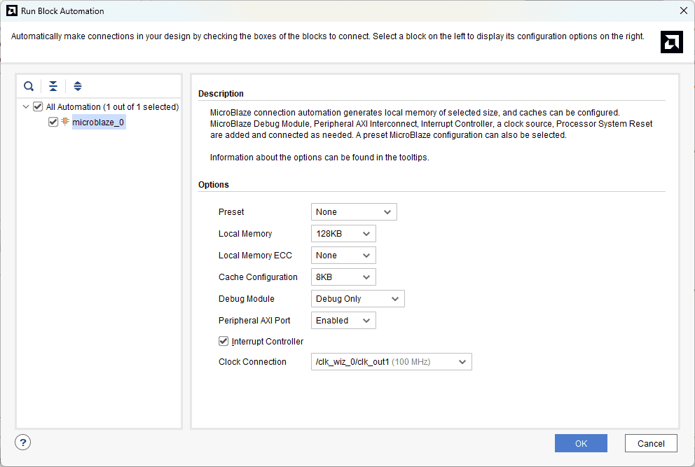
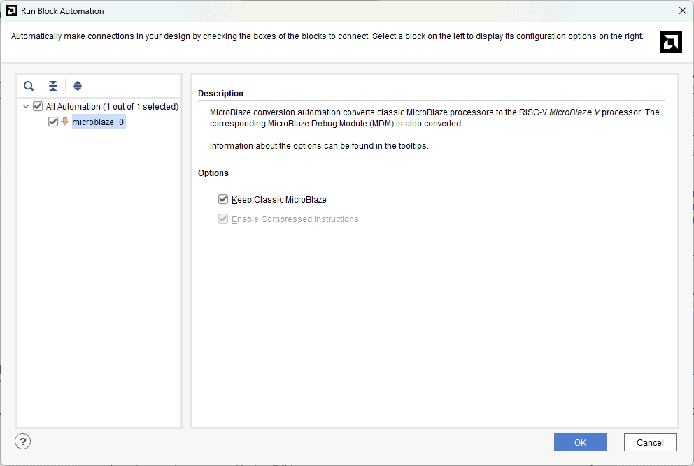
Click “OK” for Vivado to automatically configure the blocks for you. In Vivado 2024.1 after clicking on “OK” a window will appear, here you need to select “Keep Classic MicroBlaze” and then click OK to use Microblaze.
Step 9:
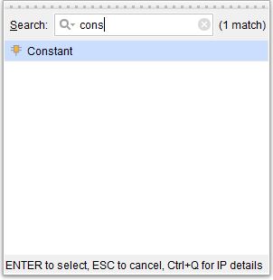
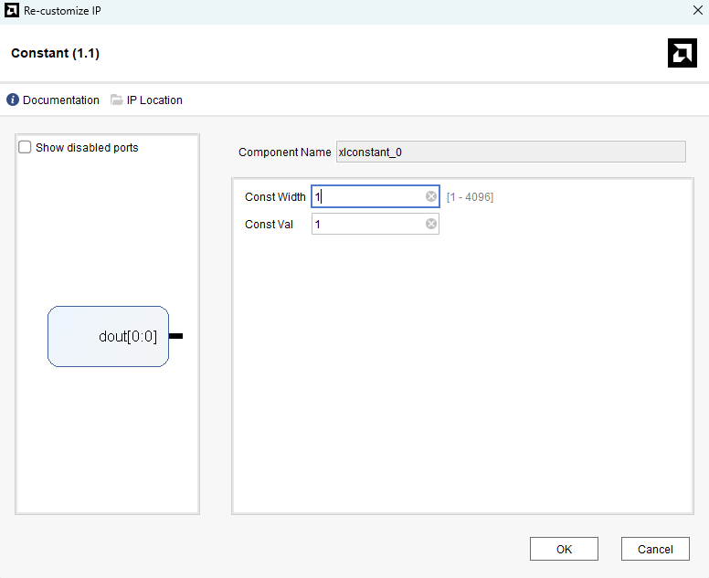
Press the “Add IP” icon and search for Constant block as shown in the image below. Drag and drop it to the Diagram window.
Double-click on the Constant block and confirm that its settings are as follows.
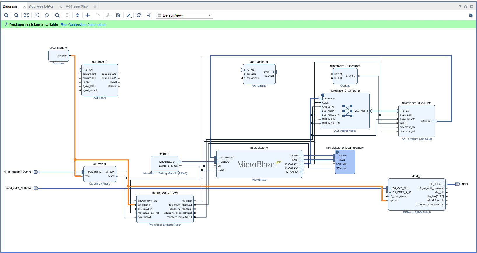
Now, connect the output of this block to reset of “Clocking Wizard”, ext_reset_in of the “Processor System Reset” and sys_rst of the “ddr4_0” block. These connections are highlighted in orange in the following image.
Step 10:
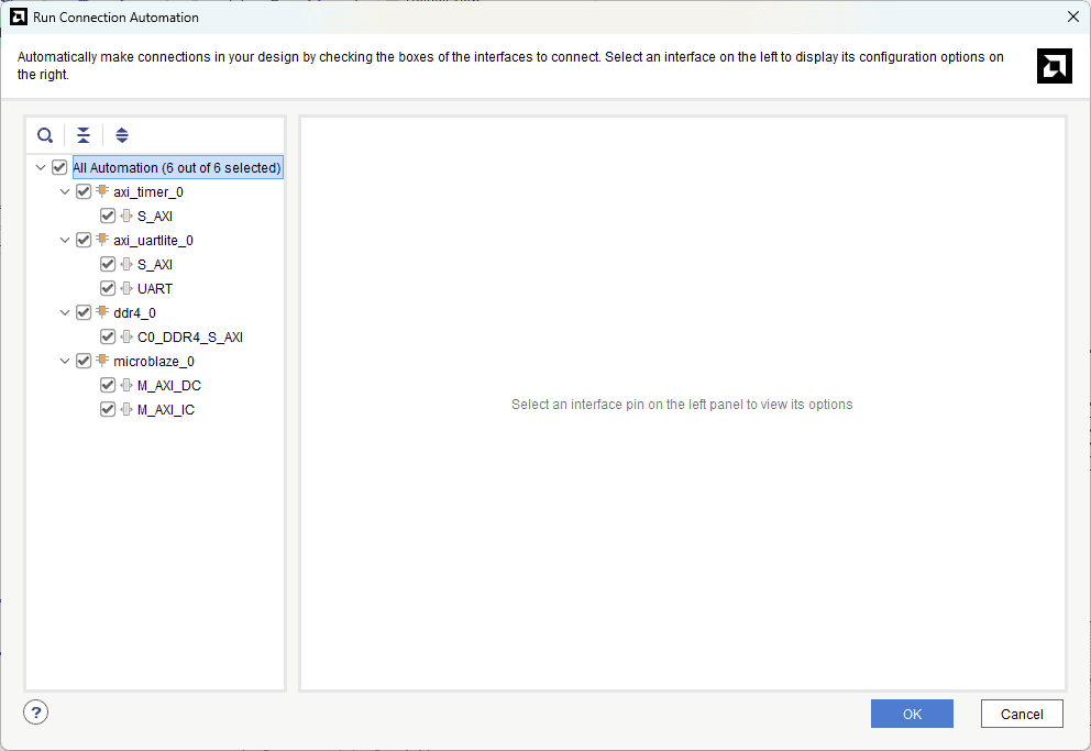
Click “Run Connection Automation” and select the “All Automation” checkbox as shown in the image below. Click “OK”.
Vivado will now connect the blocks together to make a complete system.
Step 11:
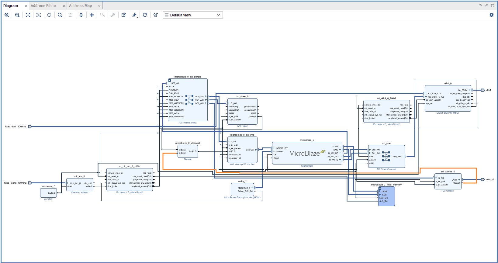
Connect the interrupts from axi_uartlite_0 and axi_timer_0 to the Concat block as shown below (the order does not matter). Make sure that the final design looks similar to the image below.
Step 12:
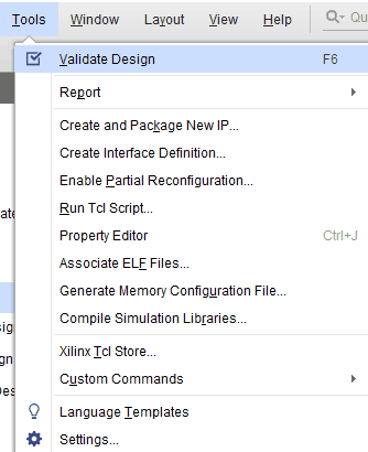
Select the “Validate Design” option from the Tools menu to ensure that the connections are correct and save the design.
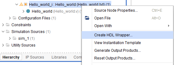
Step 13:
Right-click “Hello_world_i” in the “Sources” window, and select “Create HDL Wrapper” from the popup menu. Click “OK” on the window that appears to finish generating a wrapper.
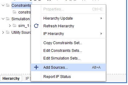
Step 14:
We have to add constraints for some ports in the design. Since we have BSP, most of the ports would be assigned from the BSP. We will have to manually assign for the rest of the ports. Right-click on “Constraints” in the Sources window, and select “Add Sources” as shown below.
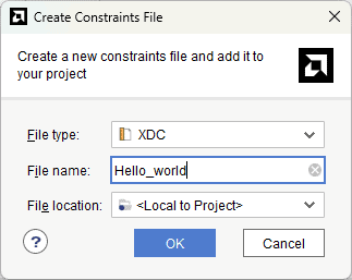
In the window that follows, select “Add or create constraints” and click “Next”. On the following page, select “Create File” and give an appropriate name to the constraints file, as shown below. Click “Finish”.
Step 15:
Copy the following constraints to the newly created constraints file and save it.
set_property PACKAGE_PIN W6 [get_ports uart_rtl_rxd]
set_property PACKAGE_PIN V6 [get_ports uart_rtl_txd]
set_property IOSTANDARD LVCMOS33 [get_ports uart_rtl_rxd]
set_property IOSTANDARD LVCMOS33 [get_ports uart_rtl_txd]
Step 16:
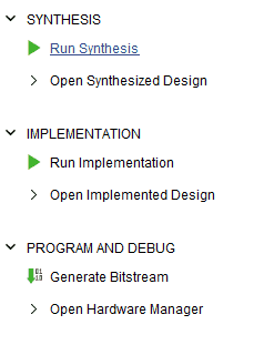
Click “Generate Bitstream” under the “Program And Debug” section to synthesize, implement and generate a bitstream.
Step 17:
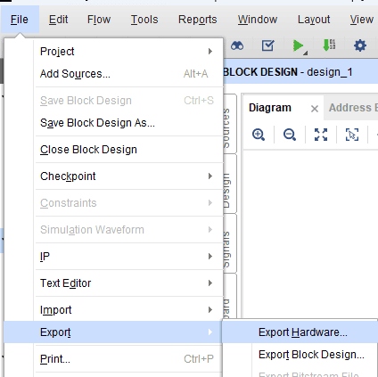
After generating the bitstream successfully, select Export -> Export Hardware from the File menu. Click Next.
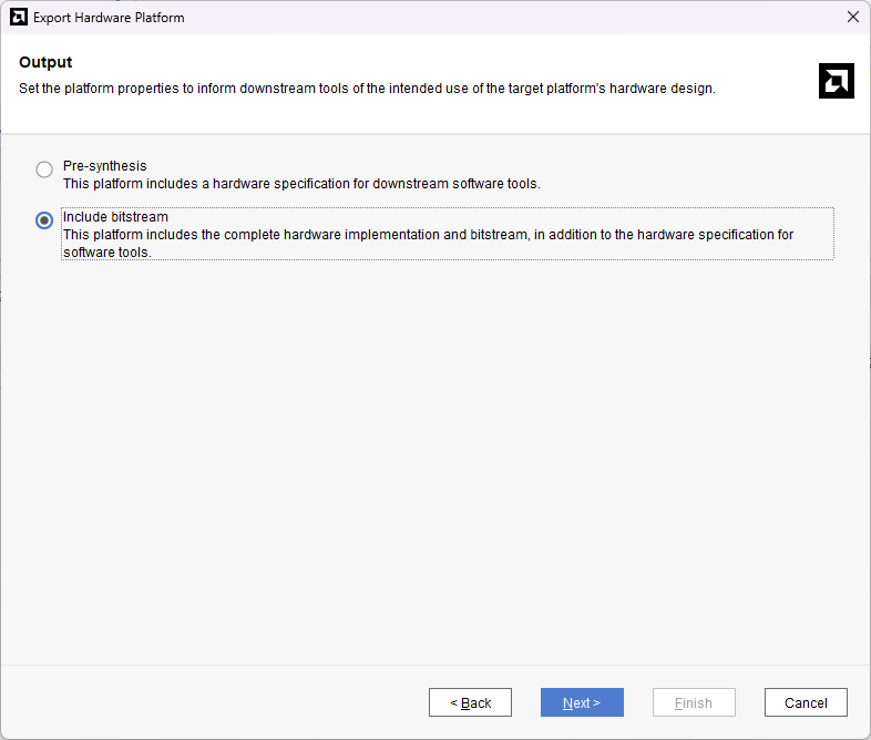
Select the “include bitstream” checkbox and click Next.
Provide the XSA file name and save it at a suitable location. Click Next and click Finish in the next dialog box.
Step 18:
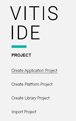
Launch Vitis IDE. In Vitis IDE window, select Create Application Project and click Next in the dialog box that appears.
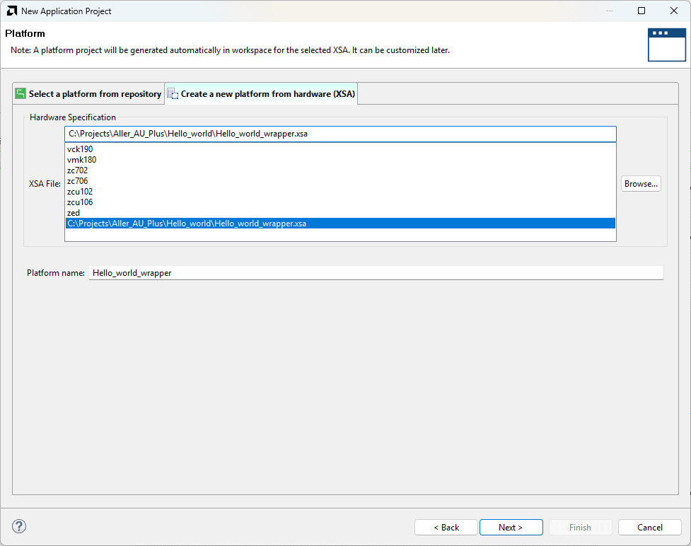
In the Platform window, select Create a new platform from hardware tab and import the XSA file which is already created (Provide XSA file location). Click Next.
Step 19:
In the Application Project Details window, give an appropriate name for the Vitis Project and click Next. Click Next in the Domain window.
Select the Hello World template from the list of available templates and click Finish.
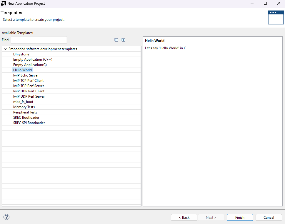
On the next page, select “Hello World” from the list of available templates and click “Finish”.
Step 20:
Once the project is created, the Vitis will automatically run a build. If that didn’t happen for any reason, run the build manually. Power up the Aller module using its carrier and connect the Xilinx Platform USB II JTAG cable for JTAG, and use a USB Type-C cable for USB-JTAG. Finally, connect the 10-pin FPC cable between the module and the carrier board.
Step 21:
Open any serial terminal program (such as PuTTY, Teraterm etc) and open the port corresponding to Aller AU-Plus with a 9600 baud rate (the default baud rate given in UART IP).
Step 22:
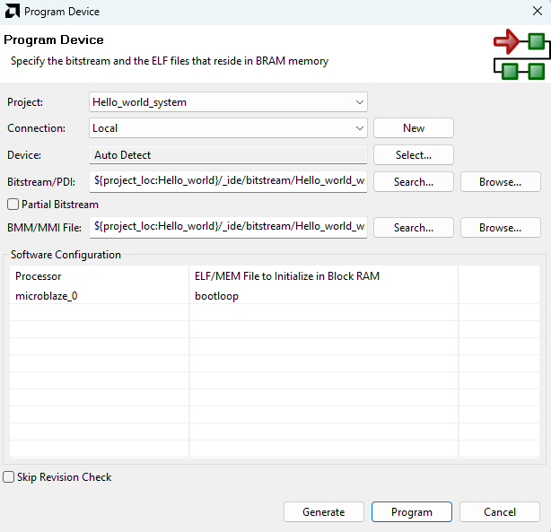
Program the FPGA on Aller with the generated bitstream and simple bootloop firmware by selecting the “Program Device” option from the “Vitis” menu.
Step 23:
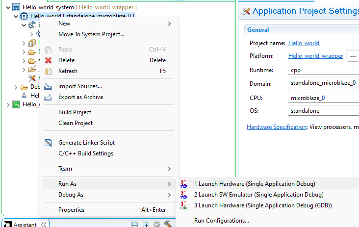
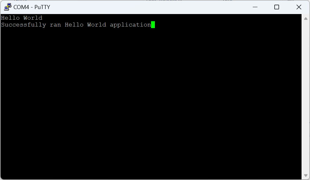
Right-click on the .elf file in the Project Explorer and select “Launch on Hardware” as shown below.
If everything went well, you will see the below output on the Serial Terminal application.
Congratulations on getting your first design running successfully on Aller!